-
-
-
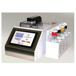
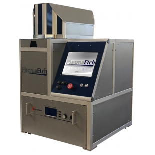
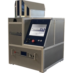
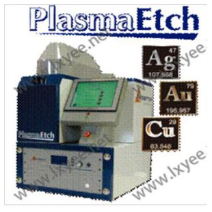
Nisene等离子芯片开封机PlasmaEtch


- 品牌:Nisene
- 型号: PlasmaEtch
- 产地:美国
- 供应商报价: 面议
-
似空科学仪器(上海)有限公司
 更新时间:2024-04-09 19:50:43
 -
企业性质授权代理商
入驻年限第7年
营业执照已审核
- 同类产品等离子芯片开封机(3件)
联系方式:张经理 4008558699转8071
联系我们时请说明在仪器网(www.yiqi.com)上看到的!
-
为您推荐

- 详细介绍
PlasmaEtch Process - 美国ZG9,548,227 B2 - 使用等离子体放电管的微波诱导等离子体。
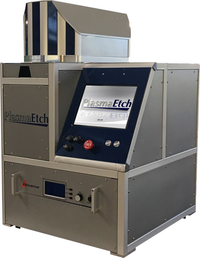
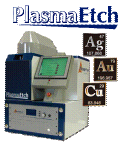
微波诱导式等离子芯片开封系统 ---- PlasmaEtch
无论是传统的金线样品,还是样品都采用铜线或银线,PlasmaEtch都能提供安全可靠的蚀刻。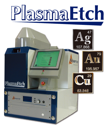 As the world moves toward more eco-friendly processes and the semiconductor manufacturing industry continues to make smaller parts with sensitive internal components, failure analysts are presented with a unique challenge: how do you etch these samples? Nisene Technology Group has bridged the gap between semiconductor manufacturing technology and failure analysis with its latest decapsulation system: the PlasmaEtch.
工作原理:The PlasmaEtch decapsulation system is a revolutionary patent-pending gas-based semiconductor etching system. Employing a never-before-seen application of microwaved gases inciting chemical radicals for isotropic etching, the PlasmaEtch is the greenest and most cost-effective etching solution available. The PlasmaEtch can etch most sample sizes, encapsulant types, and wire bond types. Whether it’s a more traditional gold wire sample, or if the sample features copper or silver wires, the PlasmaEtch delivers a safe and reliable etch.
PlasmaEtch创新点:Afterburner Downstream Focused Plasma Etching(延时激发下行聚焦离子蚀刻)
Mass Flow Control领 for All Gases(所有气体流量可控)
No Microwave Radiation Exposure to Samples During Etch Process(无微波辐射)
Low Temperature Etching(低温蚀刻)
Isotropic Etching(等向性蚀刻)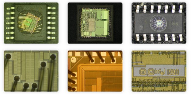
Unlike typical and less sophisticated plasma decap systems that take many hours or even days to get to the surface of the die, the PlasmaEtch can clear the encapsulant of most package types and reveal the complete die surface and wire sweep in a matter of a couple hours. Chemical-free decapsulation has never been so effective.
主要特色(Highlights):Highly Customizable Etch Recipes(高度可定制的蚀刻配方)
Etches a Wide Variety of Package Types(可蚀刻各种各样的封装类型)
Completely Chemical-free Decap(完全非化学方式蚀刻)
Eco-friendly(生态友好环保)
Touchscreen Interface(触控屏)
PC/Windows-based GUI(基于PC / Windows的GUI)
The Only Solution for Silver Wires(银线的**解决方案)
Etches Samples with All Wire Types(可蚀刻所有引线类型的样品)
Small Footprint Suited for Tabletop(桌上型紧凑尺寸机柜)- 产品优势
- 当今世界越来越关注生态友好,半导体生产工艺的持续改进则进一步导致了集成电路内部组件尺寸越来越小,也变得越来越灵敏和脆弱。由此导致了芯片失效分析的一个特定挑战:如何将样品封装去除却不会导致功能失效? Nisene公司zuixin一代的芯片开封系统为半导体生产制造技术和失效分析之间的鸿沟搭建了一座桥梁:等离子芯片开封机—PlasmaEtch Nisene科技集团有限公司从事集成电路失效分析的自动开封装置研发超过40年,拥有多项电化学及微波等离子开封机技术的ZL。
- 产品文章
-
 等离子芯片开封机PlasmaEtch
-
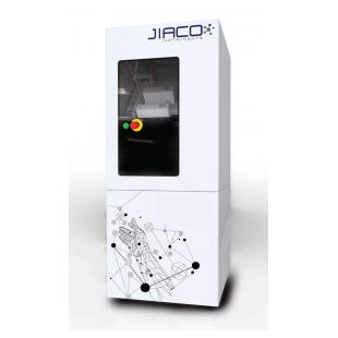 JIACO等离子芯片开封机MIP
-
 日本SAMCO RIE等离子蚀刻设备
-
 美国Nisene等离子芯片开封机PlasmaEtch
-
 美国 Nisene 等离子开封机
-
 美Nisene PlasmaEtch 等离子开封机
-
 等离子去胶机
-
 德国 PVA TePla 等离子清洗机PlasmaPen 常压等离子
-
 德国iplas微波等离子化学气相沉积 Cyrannus 1-16" 915MHz 系统
-
 NexION 350 Series电感耦合等离子体质谱仪/ICP-MS
-
 珀金埃尔默NexION® 1000G 电感耦合等离子体质谱仪
-
 NexION 1000电感耦合等离子体质谱仪ICP-MS