 冠乾科技 硅片 测试片 正片 各种规格、工艺定制
冠乾科技 硅片 测试片 正片 各种规格、工艺定制
冠乾科技 硅片 测试片 正片 各种规格、工艺定制
冠乾科技 硅片 测试片 正片 各种规格、工艺定制
冠乾科技 硅片 测试片 正片 各种规格、工艺定制
 冠乾科技 纳米压印胶 正性光刻胶 负性光刻胶 显影液 去胶液
冠乾科技 纳米压印胶 正性光刻胶 负性光刻胶 显影液 去胶液
冠乾科技 纳米压印胶 正性光刻胶 负性光刻胶 显影液 去胶液
Features
The material enables a new generation of high-performance devices with a greatly reduced size and weight footprint. The scope ranges from magnet technology for medical and research purposes to power grid protection, and includes electric generators and electric drives as well as large energy-intensive industrial processes.
Benefits
Bruker HTS Coated Conductors
Magnet technology and electric engineering require increasing quantities of quality assured and commercially processable HTS wire. Bruker EST addresses this demand with an industrial scale production of second generation YBCO-based coated conductors for application at a temperature range between 4 Kelvin and 77 Kelvin.
Tape architecture: designed for high performance
HTS coated conductors by Bruker display a multilayer architecture: stainless steel tape material of 100µm thickness serves as a substrate, or carrier, for a 1.5 micrometer (µm) buffer layer of yttria-stabilized zirconia oxide (YSZ) and a 0.05 µm buffer layer of ceramic cerium (IV) oxide (CeO2). The buffers provide both a chemical barrier and a textured surface for the deposition of a 1 µm superconducting layer of high-quality bi-epitaxial yttrium barium copper oxide (YBCO). A protecting and stabilizing 0.2 µm layer of gold or silver covers the superconducting film. The layer architecture as a whole is subsequently encased by a 20 µm copper plating serving as a shunt.
Production process: industrial quality assurance, output, and speed
In view of expanding commercial markets, HTS production at Bruker EST is based on physical deposition processes. The production technology affords uniform quality characterized by high critical currents and favorable mechanical properties of the conductor material as well as cost efficiency at high yields and throughput rates: Polished stainless steel substrate tape is cleaned before the YSZ buffer is applied by alternating beam assisted deposition (ABAD). Subsequently the CeO2 buffer and the superconducting polycrystalline YBCO layer are added by high-resolution pulsed laser deposition (HR-PLD). Applying the gold or silver film by physical vapor deposition (PVD) finalizes the layer architecture on the substrate which is then annealed and galvanic copper-plated. Dependable for commercial application
Dependable for commercial application
With its proprietary HTS production process, Bruker has mastered one of the most demanding barriers to superconductor application of a wide scope: YBCO, the brittle oxide ceramic superconductor, is fashioned into tape wire material with high critical currents which can be handled and processed in industrial environments. Stainless steel tape as a substrate provides excellent mechanic characteristics which the production process successfully transfers to the entire conductor. HTS coated conductors by Bruker EST feature a maximum tensile strength of 650 MPa and a minimum bending radius of 6 millimeters.

报价:面议
已咨询803次耗材配件

报价:面议
已咨询878次耗材配件

报价:面议
已咨询830次耗材配件

报价:面议
已咨询991次耗材配件

报价:面议
已咨询874次导体材料电阻率测试仪

报价:面议
已咨询2192次四探针方阻/电阻率测试仪

报价:面议
已咨询1764次


CosMx SMI 单细胞空间原位分子成像系统是一款具有突破性的单细胞空间原位成像平台,结合了超高分辨率成像技术和多靶标检测能力,可在单细胞和亚细胞水平对组织中的分子进行分析。

nCounter®是Bruker公司旗下nanostring公司的,系统基于数字式荧光条形码技术可对基因表达进行直接计数分析,无需反转录和PCR过程。该系统结合分子条形码和单分子成像技术可对同一个反应体系中数以百计的特定转录子进行高灵敏和高准确的检测。
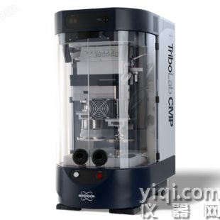
化学机械抛光研发规模的工艺研究和材料表征系统,其前身产品 (Bruker CP-4) 有超过 20 年的 CMP 领域专业知识

生物型原子力显微镜JPK NanoWizard® V BioAFM ,这是一种新型系统,标志着生命科学原子力显微镜研究的自动化和易用性的里程碑。NanoWizard V是一种非常快速的自动化 生物型AFM,可以选择与先进的光学显微镜完全集成。它能够对从亚分子到细胞和组织的大小范围内的样品进行快速、定量的机械测量和动力学分析。系统参数的自动设置、对齐和重新调整为力学生物学动态实验的长期、自我调节实验开辟了新的可能性。


