
 Human MSP ELISA Kit (人MSP ELISA试剂盒)|Beyotime/碧云天|96次
 试剂盒EpiScope MSP Kit|TAKARA|200Rxns
 MSP 试剂盒|mlbio/酶联|48T
MSP 试剂盒|mlbio/酶联|96T
MSP 试剂盒|mlbio/酶联|48T
MSP 试剂盒|mlbio/酶联|96T
 Rat MSP/MST1 ELISA Kit(大鼠巨噬细胞刺激蛋白(MSP/MST1) )|爱萌优宁|96T
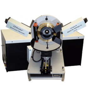
Microspectrophotometer MSP500 Introduction
Microspectrophotometer (Micro-Photometer, Micro Spectrophotometer) is used to characterize optical properties of thin films, thick coatings over a micron region area. Microspectrophotometer is also called microreflectometer, micro-reflectometer, microspectrometer, microphotometer (Spectroscopic), microspectroscopic photometer etc. With unique design by Angstrom's professionals, user can enjoy digital imaging capability in Microspectrophotometers (MSP series) by live video, powerful digital editing, measurement tools for reflection, transmission, absorption spectra. Data acquisition only takes milliseconds. TFProbe software allows user to set up heating stage or coo领 stage for kinetic study in real time for optical property changes such as reflectance, transmittance, coating thickness, refractive index (optical constants) etc. Automatic mapping function is also available in various Microspectrophotometer models with motorized X-Y stage or Rho-Theta Stage, plus the motorized focus function. Wavelength range usually is an important factor for user to consider. Angstrom's microspectrophotometer covers from deep-ultraviolet (DUV) to near-infrared (NIR) ranges. Which range 首ld be considered will depend on several factors such as what are thickness ranges for thin film or thick coating, what is typical wavelength range of interest for reflectance or transmittance and so on. MSP500 is most advanced model which covers from 250 to 1700nm large wavlength range. Selectable options, motorized mapping stage, fluorence application attachment, are available.
FEATURES:
· Easy to operate with Window based software
· Advanced optics and rugged design for highest uptime and the best system performance
· Array based detector system to ensure fast measurement
· Affordable, portable and small footprint table top design
· Measure film thickness and Refractive Index up to 5 layers over micron size region
· Allow to acquire reflection, transmission and absorption spectra in milliseconds
· Capable to be used for real time spectra, thickness, refractive index monitoring
· System comes with comprehensive optical constants database and library
· Advanced Software allows user to use either NK table, dispersion or composite model (EMA) for each individual film
· Integrated Vision, spectrum, simulation, film thickness measurement system
· Apply to many different type of substrates with different thickness up to 200mm size
· 2D and 3D output graphics and user friendly data management interface
· Advanced Imaging software for dimension measurement such as angle, distance, area, particle counting and more
· Various options available to meet special applications
SYSTEM CONFIGURATION:
· Model: MSP500RTMF
· Dual Detector System: CCD Array with 2048 pixels for UV-Vis and InGaAs Arrary for NIR
· Light Source: High Power DUV and Visible
· Stage: Black Anodized Aluminum Alloy with motorized travel distance 100mm by 75mm
· Focus: Motorized Auto focus with Joystick control.
· Long Working Distance Objectives: 10x, 15x, 50x (one DUV objective included)
· Communication: USB
· Software: TFProbe 2.4/2.5 with Fully automatic Mapping Capability and 2D/3D graphics outputs
· Measurement Type: Reflection/Transmission spectra, Film thickness/refractive index, fluorescence and feature dimensions
· Computer: Intel Core 2 Duo Processor with 200GB Hard drive and DVD+RW Burner plus 19” LCD Monitor
· Power: 110– 240 VAC /50-60Hz, 3 A
· Dimension: 16’x16’x18’ (Table top setup)
· Weight: 120 lbs total
· Warranty: One year labor and parts
SPECIFICATIONS:
· Wavelength range: 250 to 1700 nm
· Wavelength Resolution: 1nm for UV-Vis and 5 nm for NIR
· Spot Size: 100µm (4x), 40µm (10x), 30µm (15x), 8µm (50x)
· Substrate Size: up to 20mm thick
· Measurable thickness range*: 2 nm to 50 µm
· Measurement Time: 2 ms minimum
· Accuracy*: better than 0.5% (comparing with ellipsometry results for Thermal Oxide sample by using the same optical constants)
· Repeatability*: < 2Å (1 sigma from 50 thickness readings for 1500 Å Thermal SiO2 on Si Wafer)
OPTIONS:
· Wavelength extension to Further DUV or longer NIR range (~2500nm)
· Higher power optics for smaller spot size
· Customized configuration for special applications
· Heating and Coo领 Stage for dynamic study
· Optional stage size holding samples up to 300mm
· Higher wavelength range resolution down to 0.1nm
· Various filters for special applications
· Add-on accessories for fluorescence measurement
· Add-on accessories for Raman applications
· Add-on accessories for polarizing applications
· Automatic Mapping Stage up to 300mm wafer
APPLICATIONS:
· Semiconductor fabrication (PR, Oxide, Nitride..)
· Liquid crystal display (ITO, PR, Cell gap…..)
· Forensics, Biological films and materials
· Inks, Mineralogy, Pigments, Toners
· Pharmaceuticals, Medial Devices
· Optical coatings, TiO2, SiO2, Ta2O5…..
· Semiconductor compounds
· Functional films in MEMS/MOEMS
· Amorphous, nano and crystalline Si
APPLICATION EXAMPLES:
· Measured Transmission Spectra for Color Pixels
![]()
· Measured Film Thickness of TiO2 on Silicon
![]()
· Measured Reflection Spectra over a MEMS Device Inside/Outside a Via-hole
![]()
· 4. Digital Imaging Function in MSP300 System
![]()
NOTE:
· System configuration and Specifications subject to change without notice
· * Film property, surface quality and layer stack dependent
· Customized system available for special applications
· TFProbe is registered trademark of Angstrom Sun Technologies Inc.
报价:¥1
已咨询1243次MSP500

报价:面议
已咨询4503次
报价:面议
已咨询4144次拉曼光谱仪
报价:面议
已咨询8147次工艺设备

报价:¥1
已咨询1405次SR300

报价:面议
已咨询5958次拉曼光谱仪
报价:面议
已咨询4037次手持式光谱荧光分析仪

报价:面议
已咨询128次植物生理生态监测


ChroZen HPLCZ先进的技术,FlowMasterTM,通过建立一个独特的算法,在任何条件下对溶剂的压缩性补偿做出正确的预测,产生Z准确和精确的流速。这能够通过监测流量波动提供非常稳定的流量速率,并提供显著的RT重复性和区域重复性

1、 Very low noise switches非常低的噪声开关 2、 Fast switching time (35...100ns)快速开关时间(35...100ns) 3、 200V to 1000V range (更高电压可定做) 4、 10通道

1、 100K to 300K operating range 2、 Designed as Front End Stage for FT-ICR Traps 3、 2 Independend Channels 4、 Wide Frequency Range: 0.7 kHz to 30 MHz, customizable 5、 Low Noise Design 6、 Baking in Vacuum up to 125 °C 7、 is implemented as print board version and intended for direct mounting inside a vacuum setup

瑞士苏黎世仪器公司(Zurich Instruments)超高频锁相放大器UHFLI解调频率高达600MHz,采用全数字信号处理,而在整个频率范围内提供100 dB的动态存储。

苏黎世仪器公司(Zurich Instruments)HF2LI 是一款高端数字锁相放大器,信号频率响应范围扩展至50MHz,拥有两个锁相单元,在测量系统中可代替两台常规锁相放大器.


