![]()
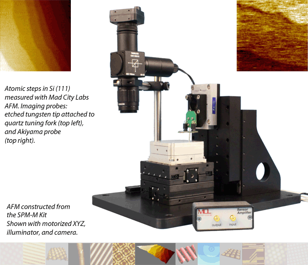
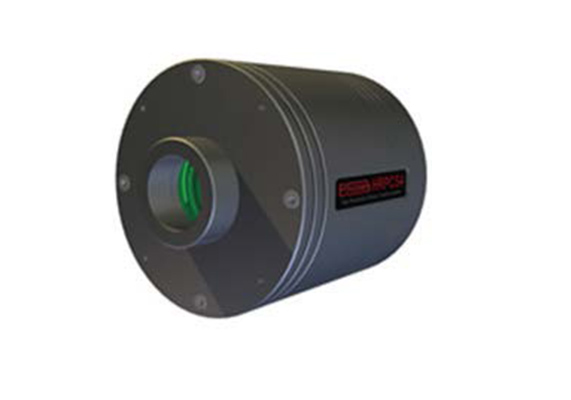
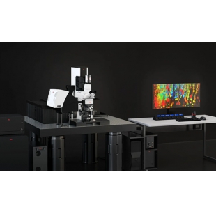
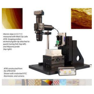
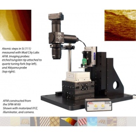
The SPM-M Kit combines the MadPLL® instrument package with Mad City Labs high resolution nanpositioning systems to form a high performance, closed loop, scanning Akiyama probe or tuning fork AFM. The seamless integration of hardware combined with the built-in automated control of MadPLL® means that you can concentrate on getting results, not tweaking parameters. Applications for the SPM-M Kit include nanoscale characterization and nanoscale fabrication applications such as optical antennas, nano-optics, semiconductors, data storage, and more. The SPM-M Kit is ideal for research and teaching laboratories offering high performance, versatility, simplicity and excellent value.At left: Schematic of a typical AFM instrument based on the SPM-M Kit.The SPM-M Kit includes: MadPLL® Instrument Packagedigital phase lock loop (PLL) controllerprobe mounting boardsfive quartz tuning forksNano-SPM200 nanopositioning stage (XY)Nano-OP30 nanopositioning stage (Z)3 axis closed loop Nano-Drive® controllerZ axis open loop/close loop switch (OCL option)AFMView™ SoftwareAFMView™ TutorialAdapter plate between probe mount board and Nano-OP30Application note: "AFM Kit with manual positioning"Application note: "Tungsten tip etching station"MadPLL® is a powerful instrument package that allows the user to create an inexpensive, high resolution resonant scanning probe microscope using Mad City Labs nanopositioning systems. The MadPLL® package includes a digital phase lock loop (PLL) controller, software, sensor amplifier board, and resonant probe mounting board. MadPLL® includes five (5) each of the vertical, horizontal, Akiyama, and blank probe boards. In addition, each unit is shipped with five (5) tuning forks. Additional probe boards and tuning forks can be purchased separately.Available options:Double walled isolation enclosureCoaxial illuminatorMotorized or manual Z-axis approachMotorized or manual XY-axisCameraSPM baseplateSPM Etch KitNot included:These items are described in the application note and are listed in the Bill of Materials (BOM)L-BracketFasteners or clampsRecommended additional items:Vibration isolation table |
|
Instant AFM - just add science!
|
Seeing is Believing!
|
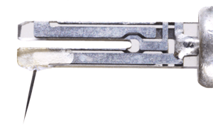 An etched tungsten tip glued to a quartz tuning fork.
|
Additional Information | ||
MadPLL® Brochure | Laser Focus World Article 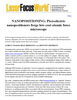 NANOPOSITIONING: Piezoelectric nanopositioners forge low-cost atomic force microscope | AFM Video Tutorial |
MadPLL® Sensor Probe Board Drawing  | Application Notes: SPM-004 "Building an AFM with motorized XYZ and camera" | |
Related Products |
|
报价:面议
已咨询1913次原子力显微镜(AFM)和近场光学显微镜(NSOM)
报价:面议
已咨询432次多光子成像

报价:面议
已咨询2587次
报价:面议
已咨询2228次
报价:面议
已咨询3203次
报价:面议
已咨询214次原子力显微镜
报价:面议
已咨询2046次原子力显微镜(AFM)和近场光学显微镜(NSOM)
报价:面议
已咨询589次多光子成像
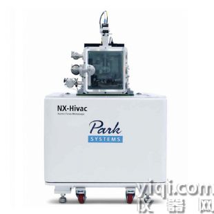
Park NX-Hivac通过为失效分析工程师提供高真空环境来提高测量敏感度以及原子力显微镜测量的可重复性。与一般环境或干燥N2条件相比,高真空测量具有准确度好、可重复性好及针尖和样本损伤低等优点。

高精度探针针尖变量的亚埃米级表面粗糙度测量,晶圆的表面粗糙度对于确定半导体器件的性能是至关重要的,对于先进的元件制造商,芯片制造商和晶圆供应商都要求对晶圆商超平坦表面进行更精确的粗糙度控制。
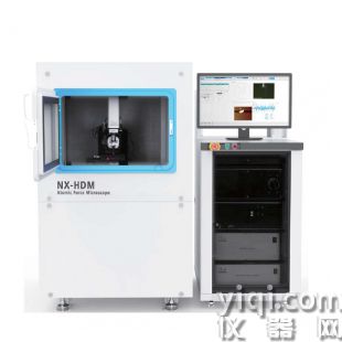
对于工程师来说,识别介质/平面基底的纳米级缺陷的任务是一个非常耗时的过程,Park NX-HDM原子力显微镜系统可以自动缺陷识别,通过与各种光学仪器的联用可以提高缺陷检测效率。
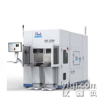
Park Systems推出NX-3DM全自动原子力显微镜系统,专为垂悬轮廓、高分辨率侧壁成像和临界角的测量而设计。
CSI是一家法国科学设备制造商,拥有专业的AFM设计概念,以及为现有的AFM提供设计选项。它避免了激光对准需要预先定位针尖的系统,针尖/样品的顶部和侧视图,结合垂直的马达控制系统,使预先趋近更加容易。
EM-AFM可在SEM中同时提供原子力显微镜成像和纳米机械测量。它综合了这两种技术的优点,可高速获得高分辨率的三维图像,并且在微纳米和亚纳米尺度上实时观察纳米级力的相互作用,与常规SEM/FIB兼容,