-
-
-
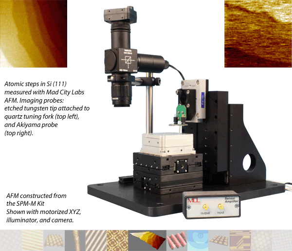
MCL原子力显微镜SPM-M套件
- 品牌:MCL Think Nano
- 型号: SPM-M Kit
- 产地:美洲 美国
- 供应商报价:面议
-
北京欧兰科技发展有限公司
 更新时间:2022-03-04 17:31:39
 -
销售范围售全国
入驻年限第9年
营业执照
- 同类产品原子力显微镜(AFM)和近场光学显微镜(NSOM)(8件)

立即扫码咨询
联系方式:400-822-6768
联系我们时请说明在仪器网(www.yiqi.com)上看到的!
-
为您推荐

详细介绍

 Introduction
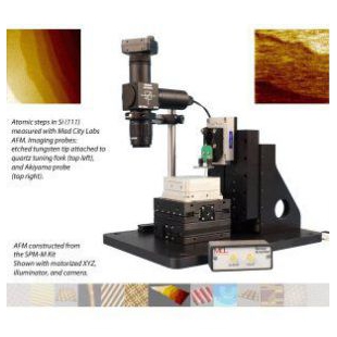
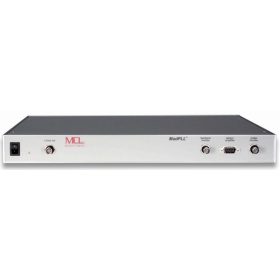
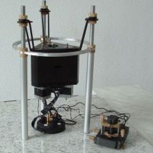
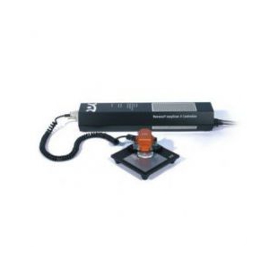
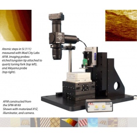
The SPM-M Kit combines the MadPLL instrument package with Mad City Labs high resolution nanpositioning systems to form a high performance, closed loop, scanning Akiyama probe or tuning fork AFM. The seamless integration of hardware combined with the built-in automated control of MadPLL means that you can concentrate on getting results, not tweaking parameters. Applications for the SPM-M Kit include nanoscale characterization and nanoscale fabrication applications such as optical antennas, nano-optics, semiconductors, data storage, and more. The SPM-M Kit is ideal for research and teaching laboratories offering high performance, versatility, simplicity and excellent value.At left: Schematic of a typical AFM instrument based on the SPM-M Kit.The SPM-M Kit includes: MadPLL Instrument Packagedigital phase lock loop (PLL) controllerprobe mounting boardsfive quartz tuning forksNano-SPM200 nanopositioning stage (XY)Nano-OP30 nanopositioning stage (Z)3 axis closed loop Nano-Drive controllerZ axis open loop/close loop switch (OCL option)AFMView SoftwareAFMView TutorialAdapter plate between probe mount board and Nano-OP30Application note: "AFM Kit with manual positioning"Application note: "Tungsten tip etching station"MadPLL is a powerful instrument package that allows the user to create an inexpensive, high resolution resonant scanning probe microscope using Mad City Labs nanopositioning systems. The MadPLL package includes a digital phase lock loop (PLL) controller, software, sensor amplifier board, and resonant probe mounting board. MadPLL includes five (5) each of the vertical, horizontal, Akiyama, and blank probe boards. In addition, each unit is shipped with five (5) tuning forks. Additional probe boards and tuning forks can be purchased separately.Available options:Double walled isolation enclosureCoaxial illuminatorMotorized or manual Z-axis approachMotorized or manual XY-axisCameraSPM baseplateSPM Etch KitNot included:These items are described in the application note and are listed in the Bill of Materials (BOM)L-BracketFasteners or clampsRecommended additional items:Vibration isolation table
 Absolute Metrology
The SPM-M Kit incorporates the Nano-SPM200and Nano-OP30with a three axis Nano-Drivecontroller for closed loop nanopositioning in X, Y, and Z. These systems incoporate Mad City Lab's proprietary PicoQ sensor technologyfor closed loop feedback control, offering significant advantages in terms of image quality, accuracy and repeatability over open loop scanners. The sensor signal from all three axes can be read during AFM scans via the analog output signal or USB, thus minimizing the effects of hysteresis, curvilinear motion, and creep that result if data are analyzed using assumed commanded positions. Using position information from closed loop sensors also eliminates the need to scan a calibration grid in XYZ before scanning every sample. Scanning with closed loop nanopositioners saves time and improves image quality. Closed loop feedback also allows the nanopositioners to move and return to commanded positions with much more reliability than open loop systems, allowing users to return to previously scanned features for further analysis.
For further information about the PicoQ sensors used in Mad City Labs nanopositioning systems, see the PicoQ sensor technology pageand our Technical Information pages.AFM Video TutorialInstant AFM - just add science!
The video at the page linked below illustrates how to use the SPM-M kit along with an Akiyama Probe, manual coarse positioners, and hardware to create a low cost, easy assembly, high resolution AFM.Mad City Labs AFM Assembly Tutorial - How to Build an "Instant" Atomic Force Microscope Image GallerySeeing is Believing!
The images below were acquired using similar configurations to the SPM-M Kit.
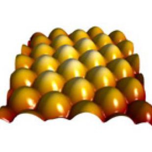
Si (111) Atomic Steps(312pm monatomic layer thickness)2μm x 2μmData taken using MadPLL with Nano-HS3 3-axis nanopositioning system and etched tungsten tip on a quartz tuning fork. Si (111) Atomic Steps(312pm monatomic layer thickness)1.76μm x 2.02μmData taken using MadPLL with Nano-HS3 3-axis nanopositioning system and Akiyama probe. Calibration grid(100nm tall lines, 2μm apart)10μm x 10μmUnidirectional scanSelf oscillation mode, constant probe signalZ force feedback: frequencyData taken using MadPLL with Nano-HS3 3-axis nanopositioning system and Akiyama probe. Calibration grid(100nm tall pegs, spaced 2μm apart)10μm x 10μmUnidirectional scanSelf oscillation mode, constant probe signalZ force feedback: frequencyData taken using MadPLL with Nano-HS3 3-axis nanopositioning system and Akiyama probe.Fly eye100μm x 100μmBidirectional scanPLL mode, constant probe signalZ force feedback: frequencyData taken using MadPLL with Nano-OP30 nanopositioning system (Z-axis), Nano-OP100 nanopositioning system (XY axes) and Akiyama probe.Human hair100μm x 100μmBidirectional scanSelf oscillation mode, constant probe signalZ force feedback: frequencyData taken using MadPLL with Nano-OP30 nanopositioning system (Z-axis), Nano-OP100 nanopositioning system (XY axes) and Akiyama probe.PMMA pattern, uncured10 μm x 10 μmBidirectional scanSelf oscillation mode, constant probe signalZ force feedback: frequencyData taken using MadPLL with Nano-OP30 nanopositioning system (Z-axis), Nano-OP100 nanopositioning system (XY axes) and Akiyama probe.Integrated circuit100 μm x 100 μmBidirectional scanSelf oscillation mode, constant probe signalZ force feedback: frequencyData taken using MadPLL with Nano-OP30 nanopositioning system (Z-axis), Nano-OP100 nanopositioning system (XY axes) and Akiyama probe.Calibration grid40 μm x 40 μmUnidirectional scanSelf oscillation mode, constant probe signalZ force feedback: frequencyData taken using MadPLL with Nano-OP30 nanopositioning system (Z-axis), Nano-OP100 nanopositioning system (XY axes) and Akiyama probe.Calibration grid(100nm tall, 10μm pitch)70 μm x 70 μmUnidirectional scanPLL mode, constant probe signalZ force feedback: frequencyData taken using MadPLL with Nano-OP30 nanopositioning system (Z-axis), Nano-OP100 nanopositioning system (XY axes) and Akiyama probe.Etched structures80 μm x 80 μmBidirectional scanSelf oscillation mode, constant probe signalZ force feedback: frequencyData taken using MadPLL with Nano-OP30 nanopositioning system (Z-axis), Nano-OP100 nanopositioning system (XY axes) and Akiyama probe.Tungsten Tip Etching with the SPM Etch Kit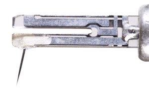
An etched tungsten tip glued to a quartz tuning fork.
One way to produce sharp probe tips suitable for building an AFM is to electrochemically etch tungsten wire. This method can produce a tip radius of better than 50nm. Post etching techniques can even sharpen the tip down to a <1nm tip radius. These sharp tungsten tips can be mounted to quartz tuning forks for AFM or for other types of scanning probe microscopy like scanning tunne领 microscopy (STM).
There are a variety of methods to choose from to etch the tungsten wire. The single lamella technique is easy to setup and can consistently produce sharp tips. Among the requirements for this process are a metallic ring, a beaker, Potassium Hydroxide (KOH), tungsten wire, and a voltage source. A drop of KOH is added to the metal ring suspended above the beaker, forming a thin film or lamella of KOH inside the metallic ring. The negative terminal of the voltage source is then connected to the suspended metallic ring. This will form the negative electrode. The beaker below the ring is then filled with KOH and the positive terminal of the voltage source is wired intod the KOH solution. This forms the positive electrode. The tungsten wire is then dipped through the center of the lamella and into the KOH in the beaker. The voltage source dis then turned on which begins the etching process. The tungsten is electrochemically etched at the lamella. The etching process automatically stops when the tungsten wire is etched so thin that the portion of wire below the lamella falls off and drops into the beaker. The remaining tungsten wire above the lamella is removed and any remaining KOH or contaminants are rinsed off with distilled water. This leaves a very sharp tip suitable for use in AFM or other types of SPM.
Mad City Labs provides an SPM Etch Kitalong with an application note on etching Tungsten tips to make this easy.Additional Information
MadPLL Brochure 
Laser Focus World Article
NANOPOSITIONING: Piezoelectric nanopositioners forge low-cost atomic force microscopeAFM Video Tutorial 
MadPLL Sensor Probe Board Drawing
Application Notes:SPM-004 "Building an AFM with motorized XYZ and camera"
SPM-005 "Building an AFM with manual XY, motorized Z and camera"
SPM-006 "Creating tungsten tips using the Mad City Labs SPM Etch Kit"
SPM-007 "Using shattered silicon as resonant probe tips"
Available upon customer requestRelated Products
SPM Accessories
MadPLL
Tuning Forks
Nano-OP Series
Nano-SPM200
Nano-HS Series
Nanopositioning Accessories
Nano-Drive
技术资料