德国Allresist 正电子束光刻胶 AR-P 6200 (CSAR 62)

描述


工艺条件
该图显示了AR-P 6200电阻的示例处理步骤。所有规范都是指导值
描述
必须适应自己的具体情况。For 进一步 信息 processing, “Detailed instructions 用于电子束电阻的ZJ处理。征求有关废水处理和一般安全的建议 instructions, ”General 产品 信息 Allresist 电子束 resists”.
等离子体刻蚀电阻
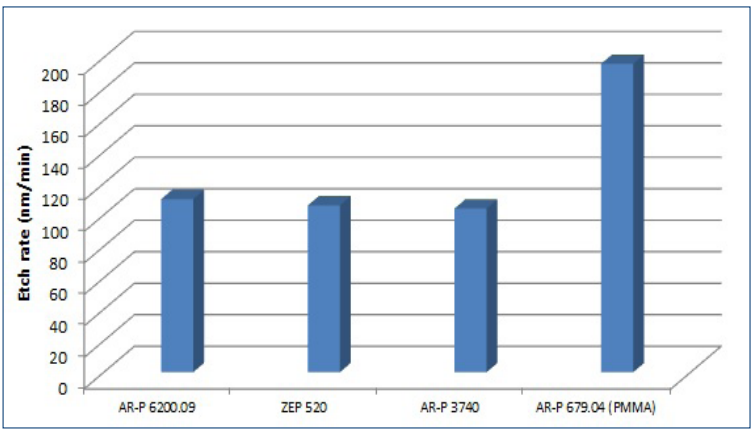
CSAR 62的特征是高等离子体刻蚀抵抗。In AR-P diagram, 等离子 蚀刻 率6200.09与的相比AR-P 3740(光刻胶),AR-P 679.04(PMMA抗蚀剂)和ZEP 520A在CF4 + O2等离子体。

处理指令
电子束照射: 所需的电子束照射剂量结构 成像 主要 取决于 所需 的 minimum 结构 size, developer, 加速度 voltage (1 - 100 kV), thickness. 和 菲林厚度。
The 照射 剂量 AR-P 6200.09 是 experiment ( CSAR 62 和 PMMA) 的 图 比较55℃/cm管(清除D0的剂量), 30 kV, 170 海里 layer, developer AR 600 - 546 , si wafer).对比是确定的14.2。
因此,CSAR 62的敏感性是the的3倍标准PMMA耐蚀剂AR- p 679.03(在AR环境下研制)600-56),或6倍以上的敏感,如果在AR 600-60. 两者之间的对比也更高,分别是2倍和1.4倍,
由于添加而增加的灵敏度增强灵敏度的成分已经在过程中发生曝光。因此,曝光后烘烤是不必要的。
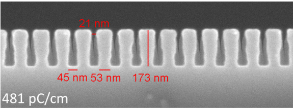
用于制备10nm沟槽(174 nm膜,100n)AR 6200.09需要的剂量约。220 pC /厘米(30kv,显影AR 600-546)
E-beam exposure: The required e-beam exposure dose for structural imaging mainly depends on the desired mi
nimum structure size, the developer, the acceleration voltage (1 - 100 kV), and the film thickness.
The exposure dose for AR-P 6200.09 was in this experiment ( diagram comparison of CSAR 62 and PMMA)
55 μC/cm² (dose to clear D0 , 30 kV, 170 nm layer, developer AR 600-546, si wafer). The contrast was determined here to 14.2.
CSAR 62 is thus 3x more sensitive as compared to the standard PMMA resist AR-P 679.03 (developed in AR
600-56), or 6x more sensitive if developed in AR 600-60. Also the contrast is higher by a factor of 2 and 1.4,
respectively. An additional increase in sensitivity due to addition of sensitivity-enhancing components occurs already during exposure. A post-exposure bake is thus not required.
For the fabrication of 10-nm trenches (174 nm film, 100npitch), AR 6200.09 requires a dose of approx. 220 pC/cm(30 kV, developer AR 600-546)。
Lift-off structures:
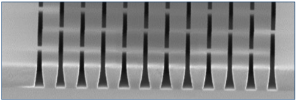
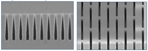
Resist CSAR 62 is well suited to generate lift-off structures with a resolution of up to 10 nm. If the dose is
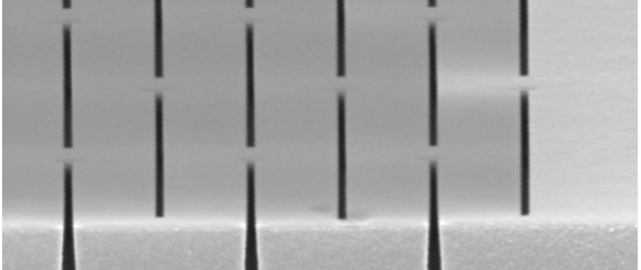
increased by a factor of 1.5 - 2, narrow trenches with defined undercut can be fabricated with AR-P 6200.09.
Undercut structures obtained with increased exposure dose
High layers for special applications:
Films with a thickness of up to 800 nm can be produced With AR-P 6200.13, and even 1.5-µm films are possible
with experimental sample SX AR-P 6200/10.

AR-P 6200.13: 100-nm trenches in 830-nm thick layer
After vapour-deposition of metal and subsequent easy lift-off, metal structures remain
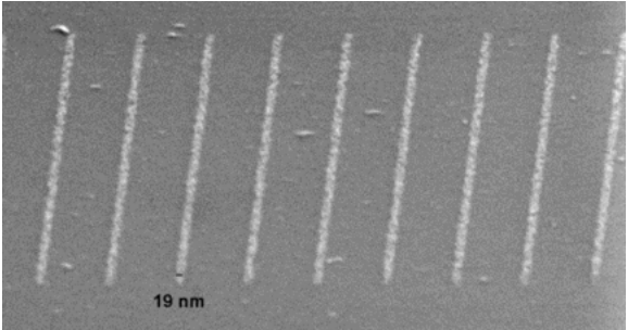
19-nm metal lines after lift-off process with AR-P 6200.09
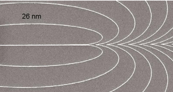
CrAu test structures with a line width of 26 nm
Another field of application for CSAR 62 is the production of mask blanks which are coated with our resist and
offered by our partners:

At a film thickness of 380 nm, 100-nm lines and spaces can be obtained on a chrome mask with AR-P 6200.13. The sensitivity is 12 µC/cm2 (20 kV, AR 600-548).
Application examples for CSAR 62
Circuits for the 5 GHz range which are primarily needed for wireless Bluetooth or Wi-Fi technologies can in future be produced with CSAR 62. E-beam lithography is also required for the research on nanomaterials like graphene, for three-dimensional integrated circuits as well as for op
tical and quantum computers. The computing power or memory density is constantly increased in each of these technologies. Applications with the highest demands on computing power (supercomputers), e.g. in computational fluid dynamics or in space applications, thus also demand microchips with highest integration density.

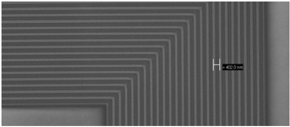
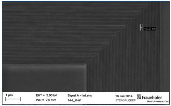
Fig. 1 CSAR 62 test structure on a mask blank with 50 nm lines and 50 nm trenches; pitch line & space here 99.57 nm
CSAR 62 for highest-resolution lithography
In the work group for nanostructured materials of the MLUHalle, CSAR 62 is mainly used in highest-resolution lithography for the lift-off and as etching mask for dry chemicaletching processes. The new resist offers several specific advantages. It achieves the high resolution of PMMA, but at amuch lower dose. Due to the high contrast, vertical resistedges are generated which allow a reliable lift-off even with thinner films and ensure a uniform lift-off up to 20 nm:

Fig. 3 Chrome structures with 20 nm lines after lift-off The goal in the lift-off of metal structures is however not
always to go beyond the limits of resolution. Typical applications for example in the contacting of nanowires rather require dimensions in a range of 30-50 nm, which can also be realised with other resists. The „resolution reserve“ of CSAR 62 however allows for significantly improved structure accuracy and faster design with less iteration:
典型的纳米线接触结构。大的区域混合了小的细节
Fig. 4 Typical structure for contacting nanowires. Large areas are mixed with small details
During dry chemical etching, for example in the structuring of silicon nitride, CSAR combines the best of two worlds: It not only allows the use as a high resolution positive resist similar to PMMA, but also offers a stability which is comparable to novolacs.
This facilitates the production of pattern with sharp edges that provide the required etch stability without the dis
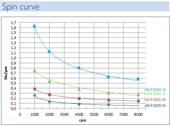
turbing faceting at the edges which otherwise occurs frequently. CSAR 62 is normally used for films with thickness values between 50 and 300 nm. Intense plasma etching for the fabrication of deep etch structures however requires significantly thicker resist layers and places special demands on resolution and contrast. Resist AR-P 6200.18 was thus designed for high layer thicknesses of 0.6-1.6 µm and is particularly well suited for the realisation of high metal structures with lift-off, deep plasma etching processes or nanowires.
Fig. 5 Lift-off structures with large undercut at a film thickness of 800 nm
薄膜厚度为800纳米时,具有大凹下的提离结构
Application examples for CSAR 62
It is nonetheless possible to produce trenches with a width of < 100 nm at a film thickness of 800 nm. The high contrast is made possible through the use of our developer AR 600-546. By increasing the irradiation dose, the degree of the generated undercut can be adjusted specifically (Fig. 5 +6). Each user can thus select the most favourable profile for his specific lift-off process.

Fig. 6 AR-P 6200.13, 823 nm layer, dose: 1440 pC/cm
Fig. 7 Vertical structures at an area dose of 120 µC/cm² for nanowires
If circles are irradiated and developed in such thick layers,columns (nanowires) can be produced due to a high metal deposition (evaporation, sputtering or electroplating) (seevertical edges in Fig. 7).
High-precision lift-off structures with the two-layer system CSAR 62/AR-P 617
The task in the IAP of the Friedrich Schiller University of Jena was to produce very small, high-precision rectangular structures. For this purpose, a two-layer system composed of AR-P 6200.09 as top layer and AR-P 617.06 as bottom layer was established. After exposure with e-beam writer Vistec SB 350OS, CSAR 62 was patterned with developer AR 600-546. The bottom layer was subsequently developed with developer AR 600-55, followed by coating with gold. The lift-off was performed with a mixture of acetone and isopropanole. The resulting structures are shown in Fig. 12. The structure sizes are 38 nm with structure intervals of approximately 40 nm. In particular to be regarded positively are the small radii of curvature at the corner of the inside of the „L“.

Fig. 12 High-precision L-shaped structures, produced with the two-layer system AR-P 6200.09 /AR-P 617.06; right 2 Layer sytems
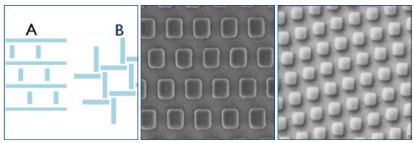
CSAR 62 – High-precision square structures
A similar objective was pursued by this working group with respect to the fabrication of square structures. The aim was again to obtain corners with particularly high resolution. Forthis purpose a CSAR 62 film with a thickness of 100 nm was irradiated with 50 kV and developed with developer AR 600-546. In addition to the excellent properties of CSAR 62,also the irradiation design is of vital importance (see Fig. 13,centre: A; right: B).

Fig. 13 Different irradiation designs and resulting square structu-res (centre: A; right: B)
CSAR 62 – Development at lower temperatures
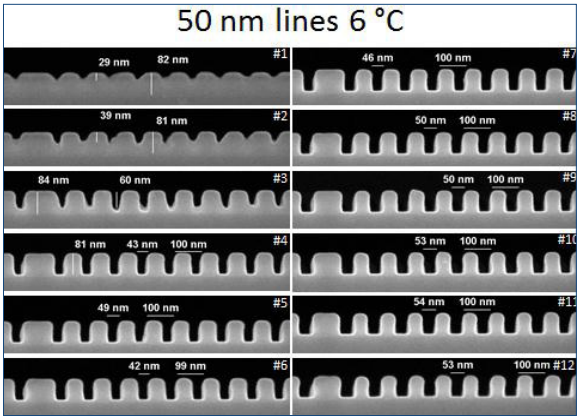
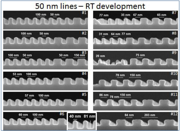
The sensitivity of CSAR 62 is strongly influenced by the choice of the developer. In comparison to the standard developer AR 600-546, the sensitivity can almost be increased tenfold if 00-548 is used which is however accompanied by an incipient erosion of unexposed resist areas. This is tolerable to a certain extent: If, for example, always 10% of the layer is lost, can this effect be compensated for in advance. Erosion can also be avoided if the development is carried out at lower temperatures, but this is again associated with a certain loss of the previously gained sensitivity. It thus comes down to the fact that an optimisation of the process is required. The lower temperatures offer, due to the more gentle development step, the possibility to increase the contrast or reduce the edge roughness.
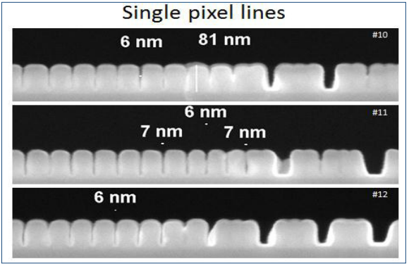
Fig. 14-16 show the sensitivities and resolutions of AR-P6200.04 at 6 °C and 21 °C (room temperature). Due to
the high contrast at 6 °C, a resolution of 6 nm could be achieved.
Application examples for CSAR 62

Fig. 14 CSAR 62 structures at 6 °C, opt. dose 195 pC/cm
Fig. 15 CSAR 62 structures at 21 °C, opt. dose 121 pC/cm
Fig. 16 Max. resolution of 6 nm at 235 pC/cm and 6 °C
CSAR 62 nanostructures written with 100 kV
At the Karlsruhe Institute of Technology, the suitability of CSAR 62 for the fabrication of complex architectures was investigated in detail. CSAR 62 layers were irradiated with e-beam writer EBPG5200Z at 100 kV and developed with developer AR 600-546. The results are shown in the figures below.

Fig. 17 SEM images (gold-sputtered): CSAR 62 nanostructures, parameters: film thickness 200 nm, dose 225 µC/cm2 , 100 kV, developer 00-546, 3 min, stopper AR 600-60。
A particular challenge is the writing and development of nano-sized hole structures. Using CSAR 62, a diameter of
remarkable 67 nm could be realised, whereby the sophis ticated structural element shows a very regular pattern.
Developer for T-gate applications with AR-P 617X AR 600-50/2 is a new, sensitive and highly selective developer for high-tempered AR-P 617 layers (SB>180 °C). PMMA or CSAR 62 layers are not attacked, which is of particular importance for multilayer processes e.g. in the manufacture of T-gates.

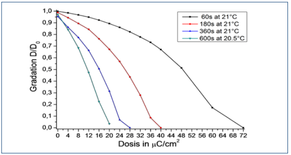
Fig. 18 AR-P 617, film thickness: ~1 µm, SB 10 minutes at 200 °C, 50kV, dose variations, dependence of the sensitivity on the development time with developer X AR 600-50/2 at room temperature, stopper AR
600-60
The sensitivity can easily be controlled via the duration of the development. At a development time of 60 s, the dose to clear is about 70 μC/cm2 , after 3 minutes of development about 40 μC/cm2 , after 6 minutes 25 μC/cm2 , and after 10 minutes about 20 μC/cm2 ! The amount of dark erosion is very low, even at longer development times.
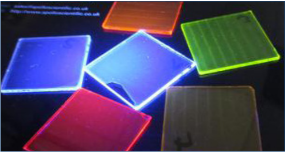
Fluorescent films with CSAR 62 and PMMA
Fluorescent dyes can be embedded into positive-tone ebeam resists like CSAR 62 and PMMA. For this purpose,
both PMMA and CSAR 62 polymers were prepared in asolvent mixture which also dissolves the fluorescent dyes
to a sufficient extent. The use of different fluorescent dyes allows a defined adjustable emission in various wavelength ranges. These dyes are highly process-stable, and structuring is performed in the same manner as in corresponding standard processes with uncoloured e-beam resists. By embedding dyes into CSAR 62, resist films could be generated which optionally show violet, blue, yellow, orange or red fluorescence. The intense fluorescence is retained even after tempering at 180 °C.
Fig. 19 Intensely fluorescing films of CSAR 62 on glass.
Fig. 20 Fluorescent structures (UV irradiation with a wavelength < 250nm, developer AR 600-546)
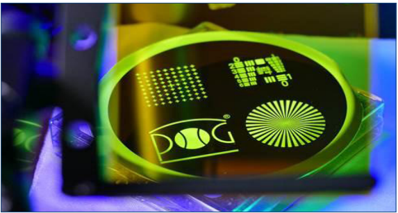
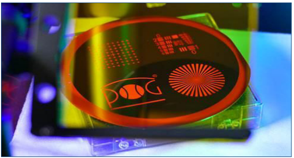
Fluorescent PMMA architectures were produced by Precision Optics Gera GmbH via electron beam lithography.
These structures could be developed residue-free using an optimized developer. If these resist structures are
excited with UV light (as shown in the two pictures), they begin to glow intensely.
Fig. 21 Yellow fluorescent PMMA-based resist architectures
Fig. 22 Red fluorescent PMMA-based resist architectures
Due to the properties of these e-beam resists, resolutions up to the 10 - 20 nm range are possible. The main field of this application is in optical industry; these materials are e.g. required for night vision devices. Fluorescent resist films are furthermore used for applications in microscopy.

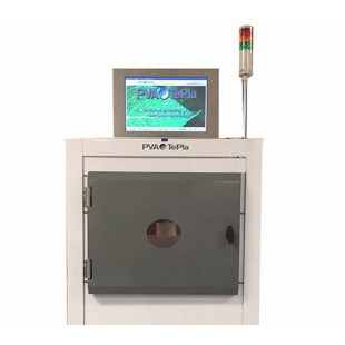 等离子去胶机IoN 100WB-40Q
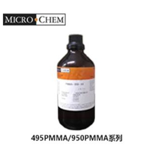 MicroChem 电子束光刻胶 PMMA
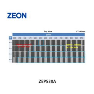 ZEON 电子束光刻胶ZEP530A
 MicroChem PMGI & LOR Lift-off光刻胶
 MicroChem 光刻胶负性光刻胶 SU-8系列

